LioniX International
  • Home
  • Photonics
    • Photonic IC Development
      • Photonic integrated circuit design
      • Photonic integrated circuit modules
      • Photonics foundry for scalable volume
    • Photonic IC technology
      • TriPleX® Silicon Nitride Waveguides
      • Photonic packaging and assembly
      • MEMS with photonics
    • MPW services
      • MPW 1550nm
      • MPW 850nm
      • MPW dates
      • Book your MPW spot!
    • Applications
      • AR/VR
      • Integrated microwave photonics
      • Optical coherence tomography
      • Optical phased arrays
      • Photonic biosensor
      • Quantum photonics
      • Ultra-narrow linewidth tunable laser
  • MEMS
    • Custom MEMS development & production
      • MEMS process development and engineering
      • Custom MEMS production and fabrication
      • MEMS services
      • MEMS Design Support
    • MEMS technology
      • Deep Reactive Ion Etching for MEMS
      • Wafer Level Packaging of MEMS
      • TriPleX® integrated photonics for optical MEMS
      • Silicon on Insulator Wafers (SOI) Processing
      • Ion Sensitive Field-Effect Transistor (ISFET)
      • Cantilevers for MEMS
    • MEMS Processes
      • LPCVD
      • PECVD Processes
      • Deep Reactive Ion Etching for MEMS
      • Lithography
      • Wet etching
      • Wafer bonding
      • Evaporation
      • Sputtering
      • Oxidation
      • Back End Processes
    • MEMS applications
      • MEMS sensors & instrumentation
      • BioMEMS
      • Inertial MEMS
      • Microfluidics
      • Micromachining
      • Optofluidics
    • MEMS Solutions
      • Bronkhorst – Gas flow sensor
      • ESA – Life Marker Chip
      • Evonetix – Synthesized DNA
      • Microsens – pH sensors with ISFET chips
      • MBARI – ISFET for deep sea pH sensor
      • Onset – Conductivity sensor
      • PerfectEdge TEM Membranes
      • SmartTip – CIPT probes
      • ThermoFisher – SEM specimen heating and biasing holder
  • Markets
    • Defense
    • Artificial Intelligence (AI)
    • Space
    • Telecom/datacom
    • Life science
    • Metrology
    • Instrumentation
  • About us
    • Blog
    • News
    • Events
    • Newsletter subscription
    • Publications
    • R&D projects
    • People
    • Work at LioniX International
  • Contact Us
  • Menu Menu
  • Silicon Nitride Waveguides

    Low Losses
    Broad wavelength range
    Mode field optimization

  • Vertical integration

    Design
    Manufacturing
    Assembly

  • Scalable Volumes

    From prototype
    to any
    Production Volume

Previous Previous Previous Next Next Next
123

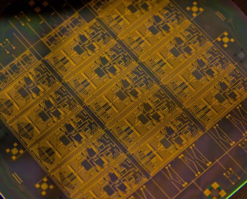
LioniX International is a vertically integrated supplier of custom photonic integrated circuit (PIC) solutions. We are an integrated photonics foundry, photonic chips design house, packaging provider, and IP developer, all rolled into one. Our proprietary technology is TriPleX® silicon nitride.

Photonic Integrated Circuits Solutions

a photonic integrated circuit development produced at LioniX

Photonic IC Development

We bring our vertically integrated capability to ensure your custom photonic integrated circuit development integrates perfectly and delivers real value in your system.
//lionix.b-cdn.net/wp-content/uploads/2022/03/Hybryd-Integration.jpg 1365 2048 jan //lionix.b-cdn.net/wp-content/uploads/2017/01/Logo-Lionix-International.gif jan2021-11-30 15:01:192025-12-15 11:12:44Photonic IC Development
Silicon nitride waveguides - triplex - used in applications requiring wide transparency ranges

TriPleX® Silicon Nitride Waveguides

Our Photonic Integrated Circuits are based on our proprietary TriPleX® silicon nitride waveguides, with ultra-low losses, wide transparency, and excellent coupling.
//lionix.b-cdn.net/wp-content/uploads/2021/12/IMG_0625-1.jpg 1365 2048 Ahmad Mohammad //lionix.b-cdn.net/wp-content/uploads/2017/01/Logo-Lionix-International.gif Ahmad Mohammad2021-07-27 14:36:552025-12-10 17:10:16TriPleX® Silicon Nitride Waveguides

Multi Project Wafer (MPW) Services

Our Multi Project Wafer services (MPW) for silicon nitride PICs gives you access to the benefits of ultra low-loss TriPleX® waveguide technology in an easy, affordable way.
//lionix.b-cdn.net/wp-content/uploads/2022/09/wafers-small.jpg 415 624 Charoula Mitsolidou //lionix.b-cdn.net/wp-content/uploads/2017/01/Logo-Lionix-International.gif Charoula Mitsolidou2016-12-06 12:13:442025-12-15 11:13:08Multi Project Wafer (MPW) Services

Photonic Chips Custom Design & Packaging

lionix international photonic integrated circuit design

Photonic integrated circuit design

We supply comprehensive expertise and facilities for the design of photonic integrated circuits as well as simulation, production, testing and characterization.
//lionix.b-cdn.net/wp-content/uploads/2022/05/GIJS8048-Edit.jpg 1366 2048 jan //lionix.b-cdn.net/wp-content/uploads/2017/01/Logo-Lionix-International.gif jan2021-10-19 15:15:162025-06-18 15:53:43Photonic integrated circuit design
a hybrid tunable laser at 850nm in a butterfly package

Photonic packaging and assembly

Make use of our in-house expertise in PIC packaging and assembly to develop an optimized, custom-made module that seemlessy integrates with your system.
//lionix.b-cdn.net/wp-content/uploads/2016/06/14pinlaser.jpg 1365 2048 Charoula Mitsolidou //lionix.b-cdn.net/wp-content/uploads/2017/01/Logo-Lionix-International.gif Charoula Mitsolidou2016-06-06 11:14:302025-12-10 17:14:38Photonic packaging and assembly
A MEMS on fabricated wafer

MEMS with photonics

LioniX International is a leading and independent supplier of customized MEMS solutions. Our expertise is product manufacturing from prototype to production volumes.
//lionix.b-cdn.net/wp-content/uploads/2021/12/GIJS8052-Edit.jpg 1366 2048 Marcel Hoekman //lionix.b-cdn.net/wp-content/uploads/2017/01/Logo-Lionix-International.gif Marcel Hoekman2016-02-28 12:41:072025-12-10 17:11:58MEMS with photonics

Integrated Photonics Modules & Systems

Applications

LioniX has deep expertise in serving communications, aerospace, defense, life science, metrology, quantum, and many other PIC application areas.
//lionix.b-cdn.net/wp-content/uploads/2019/09/OCT-Picture.jpg 908 1211 Ahmad Mohammad //lionix.b-cdn.net/wp-content/uploads/2017/01/Logo-Lionix-International.gif Ahmad Mohammad2021-11-28 21:42:452025-12-10 17:26:49Applications
a photonic integrated circuit module produced througha vertically integrated approach

Photonic integrated circuit modules

We combine cutting-edge technology, manufacturing know-how, hollistic device design, intellectual property protection, and assured reliability.
//lionix.b-cdn.net/wp-content/uploads/2022/06/IMG_4213.jpg 1365 2048 jan //lionix.b-cdn.net/wp-content/uploads/2017/01/Logo-Lionix-International.gif jan2021-10-19 15:14:262025-12-10 17:23:13Photonic integrated circuit modules
Wafer-with-optical-beamer-network-devices

Markets

We have over 20 years of experience serving clients across different integrated photonics and MEMS market sectors.
//lionix.b-cdn.net/wp-content/uploads/2024/01/3301a-SatraX-Wafer-with-optical-beamer-network-devices.jpg 1365 2048 Ahmad Mohammad //lionix.b-cdn.net/wp-content/uploads/2017/01/Logo-Lionix-International.gif Ahmad Mohammad2021-06-07 17:46:022025-12-10 17:18:49Markets

Latest

Fabrication and Assembly of an AR/VR Light-Engine Prototype in Project MatEl

31 July 2025
Read more
//lionix.b-cdn.net/wp-content/uploads/2025/07/for-the-blog.jpg 1536 2048 Sohrab Kamyar //lionix.b-cdn.net/wp-content/uploads/2017/01/Logo-Lionix-International.gif Sohrab Kamyar2025-07-31 11:59:082025-08-07 11:37:36Fabrication and Assembly of an AR/VR Light-Engine Prototype in Project MatEl
LioniX TriPleX silicon nitride external cavity laser

New Photonic Integrated Tuneable EC Laser with PZT Actuators

22 January 2025
Read more
//lionix.b-cdn.net/wp-content/uploads/2025/01/IMG_6642.jpg 1364 2048 Ilka Visscher //lionix.b-cdn.net/wp-content/uploads/2017/01/Logo-Lionix-International.gif Ilka Visscher2025-01-22 10:55:032025-08-21 11:27:54New Photonic Integrated Tuneable EC Laser with PZT Actuators
DEMUX PIC assemblyLioniX International

Reconfigurable (DE)MUX Filter for Flexible Frequency Allocation

4 November 2024
Read more
//lionix.b-cdn.net/wp-content/uploads/2024/11/Produced-4-channel-DEMUX-PIC-assembly-1.jpg 654 982 Charoula Mitsolidou //lionix.b-cdn.net/wp-content/uploads/2017/01/Logo-Lionix-International.gif Charoula Mitsolidou2024-11-04 14:34:012025-06-25 00:24:56Reconfigurable (DE)MUX Filter for Flexible Frequency Allocation
LioniX silicon nitride chip

Quantum scientists give Triplex® a HUG to entangle single photons

1 May 2024
Read more
//lionix.b-cdn.net/wp-content/uploads/2024/05/IMG_2435.jpg 1233 1817 Philip Schrinner //lionix.b-cdn.net/wp-content/uploads/2017/01/Logo-Lionix-International.gif Philip Schrinner2024-05-01 16:52:322024-05-02 13:40:34Quantum scientists give Triplex® a HUG to entangle single photons
LioniX dual hybrid InP/Si3N4 laser assembly

Want lower RF drift? Double down on laser PICs!

22 April 2024
Read more
//lionix.b-cdn.net/wp-content/uploads/2024/04/Dual-Laser-with-feedback-topview.jpg 1200 1600 Charoula Mitsolidou //lionix.b-cdn.net/wp-content/uploads/2017/01/Logo-Lionix-International.gif Charoula Mitsolidou2024-04-22 15:55:322025-04-30 15:49:26Want lower RF drift? Double down on laser PICs!
A picture of a custom packaging for a specific opto-fluidic solution for cell flow, illumination, and detection.

Optofluidic Cytometer in a TriPleX Silicon Nitride Photonic Chip

29 January 2024
Read more
//lionix.b-cdn.net/wp-content/uploads/2024/01/TriPleX-cytometer-custom-packag.jpg 771 1379 Arnoud S. Everhardt //lionix.b-cdn.net/wp-content/uploads/2017/01/Logo-Lionix-International.gif Arnoud S. Everhardt2024-01-29 03:08:162024-02-14 10:29:01Optofluidic Cytometer in a TriPleX Silicon Nitride Photonic Chip
Photo of the repeater module with the package open.

On Chip Photonic Repeater for High Throughput Satellites

18 January 2024
Read more
//lionix.b-cdn.net/wp-content/uploads/2024/01/Module.jpg 1365 2048 Ahmad Mohammad //lionix.b-cdn.net/wp-content/uploads/2017/01/Logo-Lionix-International.gif Ahmad Mohammad2024-01-18 11:12:192025-04-30 15:53:58On Chip Photonic Repeater for High Throughput Satellites
Inventing TriPleX

Waveguide Technology Innovations: The Story of the Invention (And Reinvention) of TriPleX®

13 December 2023
Read more
//lionix.b-cdn.net/wp-content/uploads/2023/12/Inventing_TriPleX.jpg 1900 2013 Marcel Hoekman //lionix.b-cdn.net/wp-content/uploads/2017/01/Logo-Lionix-International.gif Marcel Hoekman2023-12-13 11:48:072024-03-04 11:12:19Waveguide Technology Innovations: The Story of the Invention (And Reinvention) of TriPleX®
A picture of the hybrid assembly and the PCB around it.

Integrated Photonics Modules for Better Synthetic Aperture Radars

16 November 2023
Read more
//lionix.b-cdn.net/wp-content/uploads/2023/11/MicrosoftTeams-image-6.jpg 794 980 Ahmad Mohammad //lionix.b-cdn.net/wp-content/uploads/2017/01/Logo-Lionix-International.gif Ahmad Mohammad2023-11-16 14:33:012023-12-20 12:08:06Integrated Photonics Modules for Better Synthetic Aperture Radars
Minimizing coupling losses with silicon nitride waveguide tapers

Minimizing coupling losses: a multi-dimensional approach with silicon nitride waveguide tapers

19 October 2023
Read more
//lionix.b-cdn.net/wp-content/uploads/2023/10/LioniX-photonic-beamformer.jpg 1365 2048 Sadoon Al-Obaidi //lionix.b-cdn.net/wp-content/uploads/2017/01/Logo-Lionix-International.gif Sadoon Al-Obaidi2023-10-19 12:19:332023-10-25 10:10:32Minimizing coupling losses: a multi-dimensional approach with silicon nitride waveguide tapers
PreviousNext

EU Invests €15M to Help Companies Supercharge Their Products with Light

16 April 2025
Read more
//lionix.b-cdn.net/wp-content/uploads/2025/04/PhotonHub-Experience-Centre-Cleanroom-1.jpg 1367 2048 Lukas Janko //lionix.b-cdn.net/wp-content/uploads/2017/01/Logo-Lionix-International.gif Lukas Janko2025-04-16 13:23:092025-04-16 15:34:55EU Invests €15M to Help Companies Supercharge Their Products with Light
The image shows a render of LioniX new facility.

LioniX International is moving to a new purpose-built facility in Enschede, The Netherlands

9 December 2024
Read more
//lionix.b-cdn.net/wp-content/uploads/2024/12/LioniX-new-facility.jpg 1080 1737 Ilka Visscher //lionix.b-cdn.net/wp-content/uploads/2017/01/Logo-Lionix-International.gif Ilka Visscher2024-12-09 15:37:182024-12-09 15:45:47LioniX International is moving to a new purpose-built facility in Enschede, The Netherlands
Photonic integrated circuit and the module based on silicon nitride.

Cutting-edge photonics for future proof microwave communication

14 November 2024
Read more
//lionix.b-cdn.net/wp-content/uploads/2023/11/Photonic_integrated_circuit.jpg 1193 2048 Ilka Visscher //lionix.b-cdn.net/wp-content/uploads/2017/01/Logo-Lionix-International.gif Ilka Visscher2024-11-14 11:01:312024-11-14 11:57:18Cutting-edge photonics for future proof microwave communication
Photonic integrated circuit (PIC) silicon nitride MPW shuttle run from LioniX InternationalLioniX International

LioniX International secures approval to enter into bridge financing to ensure its continuity

17 July 2024
Read more
//lionix.b-cdn.net/wp-content/uploads/2024/07/Untitled-design-51.jpg 1365 2048 Ilka Visscher //lionix.b-cdn.net/wp-content/uploads/2017/01/Logo-Lionix-International.gif Ilka Visscher2024-07-17 14:49:512024-07-18 11:27:39LioniX International secures approval to enter into bridge financing to ensure its continuity
Close-up of our tunable laser in a 14-pin butterfly package.

LioniX 1310 nm laser at OFC 2024!

21 March 2024
Read more
//lionix.b-cdn.net/wp-content/uploads/2023/05/LioniX-International-Tunable-Hybrid-Laser-Package.jpg 1365 2048 Ilka Visscher //lionix.b-cdn.net/wp-content/uploads/2017/01/Logo-Lionix-International.gif Ilka Visscher2024-03-21 12:53:132024-03-21 14:13:08LioniX 1310 nm laser at OFC 2024!
Picture of Ronald Dekker, CTO of LioniX International

LioniX International appoints Ronald Dekker as new CTO

16 January 2024
Read more
//lionix.b-cdn.net/wp-content/uploads/2024/01/Untitled-design-7.jpg 988 1207 Ilka Visscher //lionix.b-cdn.net/wp-content/uploads/2017/01/Logo-Lionix-International.gif Ilka Visscher2024-01-16 10:15:332024-01-16 10:42:59LioniX International appoints Ronald Dekker as new CTO
A photo of the fully assembled and wire-bonded laser module in a 14-pin butterfly package.

Ultra-Narrow Linewidth Integrated CW Tunable Laser at 1310 nm

28 November 2023
Read more
//lionix.b-cdn.net/wp-content/uploads/2023/11/1310nm-laser-1.jpg 988 1207 Ilka Visscher //lionix.b-cdn.net/wp-content/uploads/2017/01/Logo-Lionix-International.gif Ilka Visscher2023-11-28 09:51:052023-11-28 11:12:50Ultra-Narrow Linewidth Integrated CW Tunable Laser at 1310 nm
Attendants of the first in-person BIOMED02 meeting

BIOMED02 Heralds the Future of Diagnostics

3 November 2023
Read more
//lionix.b-cdn.net/wp-content/uploads/2023/11/BIOMED-02.jpeg 826 1858 Sadoon Al-Obaidi //lionix.b-cdn.net/wp-content/uploads/2017/01/Logo-Lionix-International.gif Sadoon Al-Obaidi2023-11-03 12:08:292023-11-03 12:09:38BIOMED02 Heralds the Future of Diagnostics
Tunable external cavity laser module for Kerr freqyency comb generation

Integrated tunable laser generates Kerr frequency comb for the first time

1 August 2023
Read more
//lionix.b-cdn.net/wp-content/uploads/2023/08/LioniX-laser-Kerr-frequency-comb.jpg 600 600 Sadoon Al-Obaidi //lionix.b-cdn.net/wp-content/uploads/2017/01/Logo-Lionix-International.gif Sadoon Al-Obaidi2023-08-01 11:54:272023-11-27 23:32:06Integrated tunable laser generates Kerr frequency comb for the first time
Photo of a TriPleX MPW wafer before final dicing

TriPleX® MPW PDK Now on IPKISS

1 February 2023
Read more
//lionix.b-cdn.net/wp-content/uploads/2023/02/MPW-21-side-shallow-crop-scaled-1.jpg 1418 2048 Sadoon Al-Obaidi //lionix.b-cdn.net/wp-content/uploads/2017/01/Logo-Lionix-International.gif Sadoon Al-Obaidi2023-02-01 13:02:192023-10-20 11:12:06TriPleX® MPW PDK Now on IPKISS
PreviousNext

Photonic Integrated Circuits at LioniX International

We fabricate silicon nitride photonic chips using our proprietary waveguide technology, TriPleX®. We also design integrated photonics circuits, assemble them with optical and electronic components, package them, and provide companion electronics to control them. We carry out all of these services in-house, and can work with custom and standard formats.

Our production volume capacity is flexible to support you during the whole product development cycle. We can provide demonstrators, single-unit prototypes, photonic chip pilot runs, and small to medium volume production, all in-house. For higher volume manufacturing, we are well-connected in the integrated photonics ecosystem and have vetted expert suppliers to work with. For lower volume experiments where a full wafer is not needed, we have low cost multi-project wafer shuttle runs, with reliable building blocks and a full-option PDK.

Our silicon nitride technology, TriPleX®, maintains ultra-low propagation and coupling losses. It is uniquely capable of integrating vertical and horizontal spot size converters (tapers). It allows for heat-based and stress-based modulation without any extra optical losses. It is transparent to wavelengths from 405 nm to 2350 nm, with a fully customizable layer stack.

Our integrated photonic chips and modules are used in a suite of high-tech applications in telecom and datacom, quantum, LiDAR, biosensors, AR and VR, and other markets. We are open to work with experts in any field: you know your market, and we know our photonics. 

Get in contact with one of our photonic chips experts →

Learn more about integrated photonic chips

What are photonic integrated circuits?

Photonic integrated circuits (abbreviated to PIC or PICs) are semiconductor chips that work with light instead of electricity. They are the light-based counterpart to integrated circuits (ICs). Like ICs, PICs solve problems in innumerable fields, from computer processors to digital communication to precision sensing to automated device control to medical diagnostics.

PICs are sometimes called integrated photonics or integrated optics, which refers to the technical process by which optical systems are redesigned to fit into a chip. Optical systems rely on lenses, mirrors, and bulky electronic equipment to generate, manipulate, and detect light. These often involve optical benches, which are large, precisely manufactured tables where such optical components can be placed and moved around accurately.

Integrating such functions on chips on the scale of millimeters requires various cleanroom processing technologies, which are similar to the ones used in semiconductor manufacturing. Chemical vapor deposition, wet and dry etching, photolithography, sputtering, bonding, and many more are carried out in contaminant-free, sometimes human-free labs, to realize the devices.

How does a photonic integrated circuit work?

Photonic chips rely on total internal reflection to direct and manipulate light. Modern high speed internet uses optical fibers, which use the same physics principle. Optical fibers and photonic chips are both waveguides, because their function is to guide the direction of moving light. Light waveguides are made out of two layers, a core where the light travels freely, and a cladding which surrounds the core on all sides and reflects light. The core and the cladding work together to keep light moving only inside the waveguide.

The difference between the two technologies is that fiber optics use optical fibers as their waveguide, and integrated optics use silicon chips with waveguides built into them. Integrated waveguides are about a thousand times narrower than human hairs. Their reduced size makes integrated devices much smaller than fiber devices, and makes new designs and functions possible.

What problems do integrated photonics solve?

There are many applications where a photonic chip can outperform conventional electronic chips. Light can carry signals that are much more information-dense than electricity. Using photonic chips to process information is therefore faster and more energy efficient. For that reason, communication technologies were the first to commercialize the use of photonic integrated circuits. Light is also more sensitive to environmental changes, so photonic chips can be used as very sensitive sensors in biological applications and in quantum computing. Nothing travels faster than light, which means photonic chips can be used to make very fast distance measurements at very high accuracies. The range of applications in which photonic integrated circuits shine are only increasing more industries are exploring the possibilities of this technology.

Integrated photonics technology breakdowns from our PIC experts

Fabrication and Assembly of an AR/VR Light-Engine Prototype in Project MatEl

31 July 2025/by Sohrab Kamyar
LioniX TriPleX silicon nitride external cavity laser

New Photonic Integrated Tuneable EC Laser with PZT Actuators

22 January 2025/by Ilka Visscher
DEMUX PIC assembly

Reconfigurable (DE)MUX Filter for Flexible Frequency Allocation

4 November 2024/by Charoula Mitsolidou
LioniX silicon nitride chip

Quantum scientists give Triplex® a HUG to entangle single photons

1 May 2024/by Philip Schrinner
LioniX dual hybrid InP/Si3N4 laser assembly

Want lower RF drift? Double down on laser PICs!

22 April 2024/by Charoula Mitsolidou
A picture of a custom packaging for a specific opto-fluidic solution for cell flow, illumination, and detection.

Optofluidic Cytometer in a TriPleX Silicon Nitride Photonic Chip

29 January 2024/by Arnoud S. Everhardt
Load more

LioniX International BV

PO Box 456
7500 AL Enschede
The Netherlands

Visiting address

Building The Gallery
Hengelosestraat 500
7521 AN Enschede
The Netherlands

Contact details

Phone: +31 53 20 30 053
E-mail: info@lionix-int.com

© Copyright - LioniX International
  • Link to LinkedIn
  • Link to Youtube
  • Disclaimer
  • Privacy Policy
Scroll to top Scroll to top Scroll to top