PZT and graphene MATerials innovations for advanced opto-Electric applications in AR and biosensing
About Project MatEl:
Project MatEl is focused on combining graphene, lead zirconate titanate (PZT), aluminium scandium nitride (AlScN), semiconductors, and passive photonic circuits in TriPleX® silicon nitride chips designed for modular packaging and electronics interfacing. The project’s aim is to enable the next generation of monolithic optoelectronic integrated circuits (OEICs), with demonstrator modules planned for augmented reality and photonic biosensing.
Given the ubiquity of electronics in 21st century technology, photonic integrated circuits must always connect to and interface with the common kind of integrated circuits. The meta-integration of electronic and photonic circuits is thus a continuous goal of integrated photonics development. However, different photonic integration materials perform different functions. A pragmatic approach to maximising the functionality of photonic circuits is to combine these materials, with one material acting as the host circuit within which other materials perform essential tasks.
Between the most established photonic integrated platforms, TriPleX® silicon nitride readily exhibits core properties essential to such a host material: it has a wide transparency window (405 nm – 2.35 µm) and it has ultra low optical losses (< 0.1 db/m). The transparency allows for a wide range of applications to be implemented as integrated systems. The low losses allow for higher efficiency systems which use active photonic platforms, such as indium phosphide, or light generating semiconductors, like II-V and II-VI lasers, as the light generated by these materials can be conducted elsewhere at minimal losses. MatEl develops the TriPleX® etched pockets integration scheme to allow for the monolithic integration of graphene photodetectors and semiconductor lasers. Chip alignment and bonding will be executed using laser transfer and laser soldering, allowing for fast and accurate guest chip to host wafer assembly.
For such integration schemes to be scalable for high volume production, assembly of the chips and the packaging of the modules, especially to electronic interfaces, must be accurate, fast, and flexible for different designs. The targeted assembly approach will be wafer-level, ensuring high throughput. A modular packaging approach is also being developed in MatEl, where a generic housing allows for the host TriPleX® chip to be readily fitted and wire-bonded to external electronics.
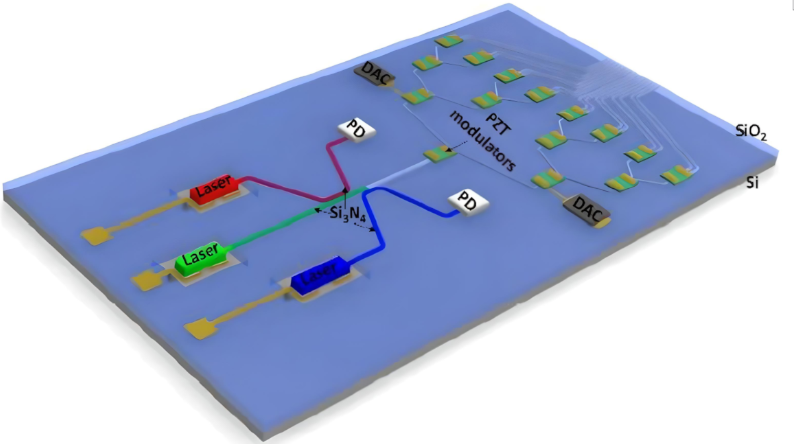
Two devices are planned in project MatEl to validate the technologies described. One is an integrated AR display, using RGB lasers and a TriPleX® demultiplexer to compose a 2D light source. The other device is a photonic Covid-19 biosensor which uses an on-chip 850 nm VCSEL and a graphene photodetector.
Schematic of the integrated augmented reality light source, featuring semiconductor laser dies integrated into TriPleX® using etched pockets and monolithically integrated photodetectors (PDs) and PZT modulators.
The Role of LioniX International:
As TriPleX® is our silicon nitride specialty, we are responsible for its development and fabrication for project MatEl. Hence, we are participating in every stage of the device development. This involves defining an architectural design for the circuits which takes into account the wafer-level hybrid integration scheme described above, including the circuit designs required for augmented reality and biosensing devices. These designs will use different TriPleX® waveguide types optimized for these applications, building up to specific circuitries and pockets for hybrid materials. We will also advice and work on the processing of the advanced materials, including graphene, PZT, and AlScN.
The wafer-level hybrid integration scheme involves its own development, which are required for the planned devices. We will advise on the laser-based methods for transfer and soldering of guest chips. New cleanroom processes are to include microstructures for wafer-level testing of integrated components. The optoelectronic performance of the graphene-based photodiodes used for light detection will also be characterised in our labs. New schemes for wafer dicing, particularly designed for chip-loaded TriPleX® will also be devised for project MatEl. We will also advise on the development of electronic components for device testing.
Further information:
🌐 Visit project MatEl’s website for a full rundown of its aims and consortium members.
🌐 Read the project’s first press release!
🌐 Stay up to date about the project by following its LinkedIn and Twitter channels.
🌐 Read more about our custom assembly and packaging services.


