About Project FLEXIT:
FLEXIT aims at streamlining the production process of photonic integrated circuit (PIC) chips and modules by better connecting the companies that constitute its production nodes. The production of PICs goes through several steps, each being the function of different enterprises. These can be broadly categorized as design, processing, assembly, packaging, testing, and analysis. Standardization of chip and module layouts, accurate and simple assembly processes, and wafer-scale testing are the next steps towards PIC mass production.
Critical to this streamlining is the design and implementation of a generic solution for the assembly and packaging of photonic chips. Optical signals require very accurate alignment between signal-carrying components (on the order of less than 100 nm) to avoid significant signal losses. For the most part, this work is currently done manually and on a case-by-case basis, such that the assembly and packaging of chips can cost four times as much as the production of the chip itself.
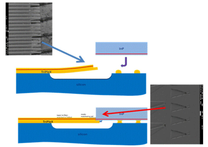
FLEXIT’s strategy to reduce these costs is to establish flexible standard assembly techniques and the use of chip-to-chip and fiber-to-chip self-aligning procedures. To develop these techniques and procedures, a composite device with an indium phosphide (InP) chip, a silicon nitride (SiN) chip on the TriPleX® platform, a CMOS semiconductor controller chip, fiber connectors, and electrical connectors will be used as a test case. For the assembly of InP and SiN, interlacing sections of both chips will reduce the required alignment accuracy from 100 nm to 2 µm while allowing for an automated pick-and-place machine to take care of the assembly. This method will allow for faster, higher yield assembly with substantially lower cost and higher throughput.
Diagram of the proposed silicon nitride and indium phosphide integration method, using interlacing ‘fingers’ and ‘facettes’.
Wafer level testing equipment will be developed for InP chips, such that electronic and photonic functions are measured simultaneously for each component. The SiN ‘fingers’ intended for the interlacing sections of the assembly will also undergo wafer-level inspection using the new equipment. Another machine will be used to select the properly-fabricated chips and separate them from the wafer. Two existing products can already be used to test these methods and their components and production processes will be redesigned to use them. Data collected from these tests will be analysed to implement smart production optimizations and logistics control. At the same time, design tools which incorporate the FLEXIT assembly method will be developed. These tools will be added to existing Computer Aided Design software for easy use.
The role of LioniX International:
As the project’s TriPleX® supplier and SiN advisor, we are participating in the design, fabrication, processing, assembly, and data gathering activities. The FLEXIT design tool which will supplement existing design tools will be tested in designing new versions of existing products. We will design and optimise fabrication processes for the SiN structures required for the interlaced assembly method to ensure high quality, voluminous yield. We will also deliver characterisations and testing specifications of these structures and test out the machine developed to carry out these processes. For electronic integration, we will help develop processes of CMOS chips and electrical connector mounting on SiN and assess their reliability. We will advise on the development of the pick-and-place assembly process as well as the chip-from-wafer selection and separation processes. The data generated from these tests will be delivered to other partners for processing.
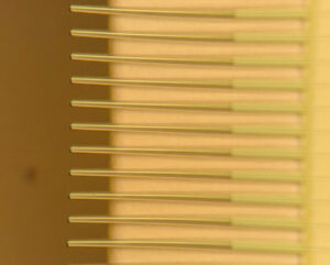
Microscope image of the TriPleX® fingers after fabrication and post-processing.
Further information:
🌐 Download the project brochure detailing all partners and their roles.
🌐 Visit the project page at Holland Semiconductors.
🌐 Visit the project page at Workfloor.
🌐 Visit the project page at Chilas.
The project is funded by the European Regional Development Fund through the OP Oost program.


