Fabrication and assembly of an AR/VR Light-Engine prototype in project MatEl
A colleague pointed this out to me at the lunch table the other day: AR/VR and space applications make the same demands to photonic chips. Both applications want smaller devices that are lighter and more power efficient. So, if someone’s got stars in their eyes, that just might be an alternative reality extraterrestrial technology!
Unlike space, AR/VR devices have a major requirement which most commercial applications share: components need to be cheap. If AR glasses are to become a consumer product, they cannot cost as much as satellites. That means scalable production. That means using reliable processes that can be easily ramped up. Ironically, this makes developing devices for AR/VR easier: designs can be immediately disregarded if there are no feasible scalability routes for them. It also means that part manufacturers, from the PICs to the diodes to the system integrators, need to maintain close collaboration to make sure the entire production line is reliable and scalable.
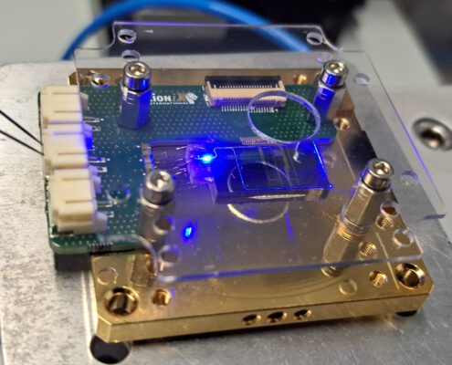
Under these constraints, we have been working with a fantastic consortium in project MatEl to take some giant leaps. One prototype has already been produced and is currently being characterized by the end-users at Creal. This first prototype had a few simple things to demonstrate. Well, individually simple tasks, but combined, they become quite tricky. Can a photonic chip produce full-spectrum visible light, split it 16 ways, have each branch get an arbitrarily chosen color, and selectively output each branch separately? We can now reliably answer: yes. Using only standard processes in our library, we managed to make the device pictured below.

The full assembly of the AR/VR prototype is demonstrated. Using a custom PCB, the chip is assembled with all components on a submount. The diodes and heaters are then wirebonded onto the PCB to drive the functional chip electronically. In this picture, the modulation of the blue diode is shown.
High-power RGB diodes were edge-coupled to our TriPleX® silicon nitride PIC. Each of these laser diodes can output at least 120 mW. As such, they can also get pretty hot. So, we placed the diodes on aluminum nitride (AlN) thermal sink submounts. The coupling loss across the interface was around 2 dB. Fans of our hybrid integration will know that this is a disappointing result for us (under 1 dB/facet is what we are used to). It highlights the importance of close collaboration for us—due to missing info about the diodes, we were unable to optimally integrate them to our PIC. Quality control across the supply chain is crucial for scalability. It is acceptable in early prototypes to have some leeway as things are getting tested out, but without reliability, there is no scalability.
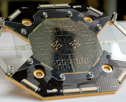
The TriPleX® chip had a circuit of combiners to mix the RGB colors, splitters that branched out to 16 channels, and directional couplers to adjust the color in each channel. Next, a variable optic attenuator array (made using Mach-Zehnder Interferometers), allowing us to adjust the output light power per channel. Finally, to outcouple each channel out-of-plane, 16 waveguide-level mirrors were fabricated with focused ion beam (FIB).
As usual, all the processing and assembly were done in-house at LioniX.
I should highlight here what really contributes to production scale-up. As with any early prototype, you never want to spend a lot of time trying to make many untested technologies demonstrate a new device. The first iteration should mostly use known quantities: reliable processes, well-tested designs, and familiar components. Edge coupling is relatively slow for hybrid integration, but it is a high-performance, well-known technique for us. Especially when using high-power diodes, it is better to rely on a low-loss integration technique so we can test the diode and circuit performance in the final demonstrator itself. The two “dependent variables”, so to speak, are the and the FIB mirrors.
The AlN submounts were a real relief. Because visible laser diodes (the bigger the better) generate so much heat, we had to keep the high-power diodes cool to keep them going at full strength. AlN is a great heat conductor. It is also nice to work with and super easy to adapt to any shape we want, which made it a perfect interposer between our standard copper submounts and the new diodes. Those will definitely speed up module production when volume is needed. The same goes for the FIB mirrors. After some tinkering with the process design, we are now able to easily add these to our TriPleX® silicon nitride waveguides. Having a scalable out-of-plane coupling option is very useful for a lot of applications that need a projection solution. An array of 16 mirrors was chosen for this design, but in fact, we could put hundreds of these in the PIC. I cannot imagine what you would make with that ability, but we are always surprised by the creativity of our clients!
So, the RGB diodes push light into the silicon nitride, the light is combined and split up, each split channel is independently tuned for wavelength and intensity, then the light is pushed out broadside. How could this be done better?
Well, for one, all tuning on this module is done with heaters. Thermo-optic actuation is fine, but stress-optic actuation is finer. For a power-sensitive application like AR/VR, piezoelectric actuators are a much better fit, since they consume negligible power in steady-state operation. Another easy upgrade is to flip-chip the diodes on the TriPleX®, instead of edge-coupling them. That speeds up the assembly considerably and enables parallelization, great for volume production. There are a couple more tricks we are working on that we cannot talk about just yet, but there is an obvious problem here that PIC designers will enjoy. How do you split light in a way that reuses power in unused channels?
We have already been working on the next demonstrator module, and we have some pretty good answers and some pretty interesting questions. We can already say that Mark II will be smaller, produce less heat, be more power efficient, and get considerably lighter. All great things for the stars, whether they are satellites or the ones who will wear cool AR glasses all day.

Sohrab received his B.Sc. degree in Advanced Technology and his double M.Sc. degrees in Applied Physics and Nanotechnology at the University of Twente. After graduation, he joined Solmates as an R&D Engineer working on improving PLD technology for large scale wafer deposition of Scandium doped Aluminum Nitride. In 2023, he joined LioniX International as a project leader, where he leads the MatEl project.
Read more:
🌐Microwave photonics development at LioniX International.
🌐LioniX Multi Wafer Project (MPW) services.
🌐 Monthly updates on our developments and events via our newsletter!
More articles from LioniX International experts:
 https://www.lionix-international.com/wp-content/uploads/2025/07/for-the-blog.jpg
1536
2048
Sohrab Kamyar
https://www.lionix-international.com/wp-content/uploads/2017/01/Logo-Lionix-International.gif
Sohrab Kamyar2025-07-31 11:59:082025-08-07 11:37:36Fabrication and Assembly of an AR/VR Light-Engine Prototype in Project MatEl
https://www.lionix-international.com/wp-content/uploads/2025/07/for-the-blog.jpg
1536
2048
Sohrab Kamyar
https://www.lionix-international.com/wp-content/uploads/2017/01/Logo-Lionix-International.gif
Sohrab Kamyar2025-07-31 11:59:082025-08-07 11:37:36Fabrication and Assembly of an AR/VR Light-Engine Prototype in Project MatEl
 LioniX International
https://www.lionix-international.com/wp-content/uploads/2024/11/Produced-4-channel-DEMUX-PIC-assembly-1.jpg
654
982
Charoula Mitsolidou
https://www.lionix-international.com/wp-content/uploads/2017/01/Logo-Lionix-International.gif
Charoula Mitsolidou2024-11-04 14:34:012025-06-25 00:24:56Reconfigurable (DE)MUX Filter for Flexible Frequency Allocation
LioniX International
https://www.lionix-international.com/wp-content/uploads/2024/11/Produced-4-channel-DEMUX-PIC-assembly-1.jpg
654
982
Charoula Mitsolidou
https://www.lionix-international.com/wp-content/uploads/2017/01/Logo-Lionix-International.gif
Charoula Mitsolidou2024-11-04 14:34:012025-06-25 00:24:56Reconfigurable (DE)MUX Filter for Flexible Frequency Allocation
