
LioniX International
  • Home
  • Photonics
    • Photonic IC Development
      • Photonic integrated circuit design
      • Photonic integrated circuit modules
      • Photonics foundry for scalable volume
    • Photonic IC technology
      • TriPleX® Silicon Nitride Waveguides
      • Photonic packaging and assembly
      • MEMS with photonics
    • MPW services
      • MPW 1550nm
      • MPW 850nm
      • MPW dates
      • Book your MPW spot!
    • Applications
      • AR/VR
      • Integrated microwave photonics
      • Optical coherence tomography
      • Optical phased arrays
      • Photonic biosensor
      • Quantum photonics
      • Ultra-narrow linewidth tunable laser
  • MEMS
    • Custom MEMS development & production
      • MEMS process development and engineering
      • Custom MEMS production and fabrication
      • MEMS services
      • MEMS Design Support
    • MEMS technology
      • Deep Reactive Ion Etching for MEMS
      • Wafer Level Packaging of MEMS
      • TriPleX® integrated photonics for optical MEMS
      • Silicon on Insulator Wafers (SOI) Processing
      • Ion Sensitive Field-Effect Transistor (ISFET)
      • Cantilevers for MEMS
    • MEMS Processes
      • LPCVD
      • PECVD Processes
      • Deep Reactive Ion Etching for MEMS
      • Lithography
      • Wet etching
      • Wafer bonding
      • Evaporation
      • Sputtering
      • Oxidation
      • Back End Processes
    • MEMS applications
      • MEMS sensors & instrumentation
      • BioMEMS
      • Inertial MEMS
      • Microfluidics
      • Micromachining
      • Optofluidics
    • MEMS Solutions
      • Bronkhorst – Gas flow sensor
      • ESA – Life Marker Chip
      • Evonetix – Synthesized DNA
      • Microsens – pH sensors with ISFET chips
      • MBARI – ISFET for deep sea pH sensor
      • Onset – Conductivity sensor
      • PerfectEdge TEM Membranes
      • SmartTip – CIPT probes
      • ThermoFisher – SEM specimen heating and biasing holder
      • University of Strasbourg – MEMS Microfluidic Optical Cavities
  • Markets
    • Defense
    • Artificial Intelligence (AI)
    • Space
    • Telecom/datacom
    • Life science
    • Metrology
    • Instrumentation
  • About us
    • Blog
    • News
    • Events
    • Newsletter subscription
    • Publications
    • R&D projects
    • People
    • Work at LioniX International
  • Contact Us
  • Menu Menu
Home » About us » Blog » Wafer-Level Optical Characterization: Improving Chip Selection Through Yield Analysis

Wafer-Level Optical Characterization: Improving Chip Selection Through Yield Analysis

As photonic integrated circuits (PICs) continue to grow in complexity, wafer-level optical characterization is becoming increasingly important for verifying chip performance before dicing. For customers, knowing which chips are functional at this stage can make a significant difference in how efficiently they are selected for further processing.

At LioniX International, we are developing optical characterization solutions that bring testing from the individual chip level to the wafer level. By measuring chips across a wafer, we can gather the data needed for yield analysis and support automated chip selection, reducing the need to characterize each chip individually after dicing.
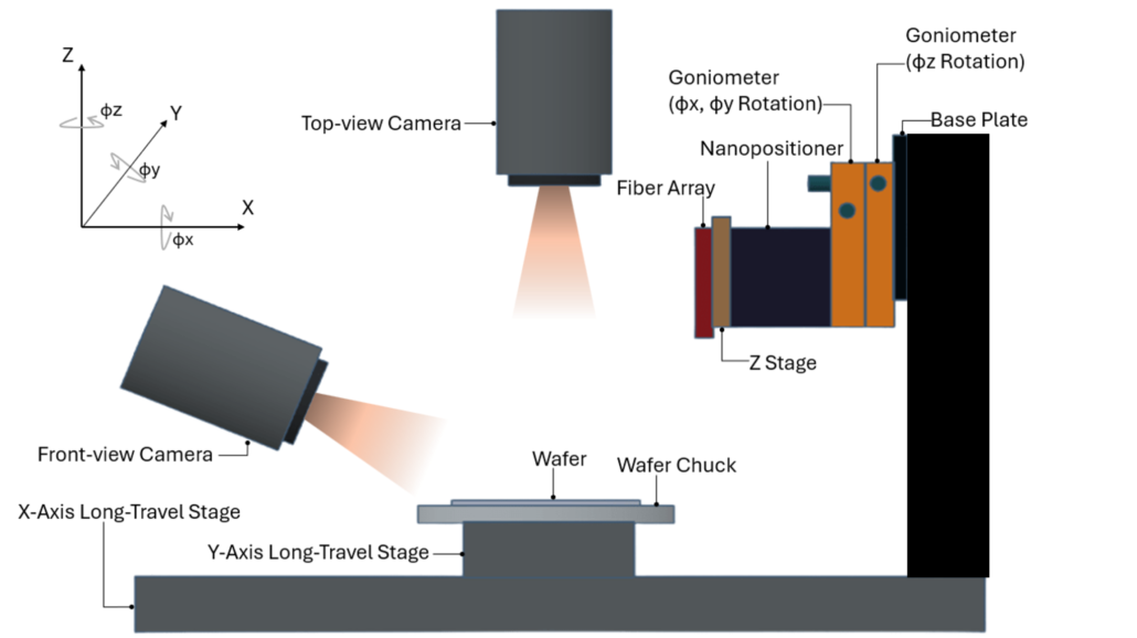
Schematic Optical Characterization Machine Setup

Schematic Optical Characterization Machine Setup

Why Wafer-Level Characterization?

Traditionally, our process control with optical characterization has been performed on one or two chips after they have been diced from the wafer. Since dicing is a destructive and expensive process, wafer-level rework is no longer possible, and resources are wasted. This approach provides only limited information about the performance of the remaining chips.

Wafer-level optical characterization allows us to measure not only test chips but also functional chips before dicing and assess their optical performance against predefined specifications. This provides a more complete picture of wafer-level yield and helps identify which chips meet the required criteria.

Designing for Testability

Wafer-level characterization does not start when a wafer reaches the test bench. It starts during the design phase.

To enable optical characterization at wafer level, photonic integrated circuits need to be designed with testing in mind. Depending on the application, this may involve incorporating grating couplers into functional chips or including dedicated test structures that allow key optical parameters to be measured before dicing.

This Design for Test approach is becoming increasingly important as the photonics industry moves towards higher-volume manufacturing. Considering testability early in the design process helps provide the optical access required for wafer-level characterization.

Wafer-Level Characterization in Practice: Lab on Chip

An example of our progress in wafer-level optical characterization is the NXTGEN | Lab on Chip project, in which we developed and demonstrated an optical characterization setup capable of measuring all chips across a wafer.

The setup combines optical measurements with chip-to-chip alignment, achieving an interval of 11 seconds between consecutive chips, including alignment and full spectral characterization of all functional channels, including Free Spectral Range and Extinction Ratio extraction. In this complete measurement run, 106 chips were characterized in 30 minutes, providing detailed information about the optical performance of the characterized chips.
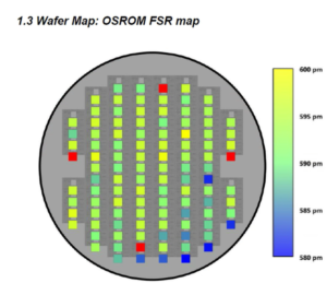
Wafer Map: OSROM FSR Map
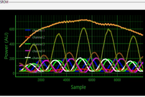
Spectra

Spectra

Tailored Characterization Solutions

Every photonic application has its own measurement requirements. Together with our partner Surfix, we developed a dedicated optical characterization process for assessing the quality of their specialized photonic biosensor chips. The functionality of these sensors comes alive only in liquid environments, and in this collaboration, Surfix has developed a coating mimicking the water environment while simultaneously being compatible with the characterization equipment.

For customers with different characterization requirements, we can explore the development of customized solutions tailored to their applications.
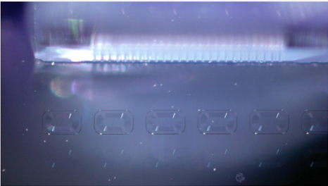
Camera view
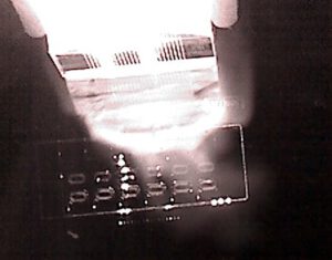
              Camera view: Coupled light

Let’s Explore the Possibilities Together

Wafer-level optical characterization offers a way to evaluate chip performance before dicing, making it easier to determine which chips meet the required specifications.

Whether you’re interested in wafer-level yield analysis or have a specific optical characterization challenge, we’d be happy to discuss your requirements and explore what is possible for your application.

Contact us to learn more about our optical characterization capabilities.

Get in touch with our experts

Philip Schrinner

Dr. Philip P.J. Schrinner started his scientific career at the (RWTH) Aachen University, where he received his B.Sc and M.Sc in the field of quantum/nano technology. To further deepen his background and to research in the field of integrated optics, he proceeded with his PhD at the University of Münster (WWU). After designing, fabricating and characterizing hybrid quantum light sources in photonic integrated circuits in the university cleanroom and labs, he joined Lionix International in 2021. In addition to developing new hybrid photonic assemblies, he is now the project leader for several commercial, national and EU projects.

More articles from LioniX International experts:

LXI & HHI intensify collaboration of their PIC platforms

27 July 2017
Read more
https://www.lionix-international.com/wp-content/uploads/2017/07/Narrow-Linewidth-Tunable-Laser.jpg 1365 2048 Marcel Hoekman https://www.lionix-international.com/wp-content/uploads/2017/01/Logo-Lionix-International.gif Marcel Hoekman2017-07-27 10:36:282017-07-27 14:06:21LXI & HHI intensify collaboration of their PIC platforms

Record-low linewidth laser

4 July 2017
Read more
https://www.lionix-international.com/wp-content/uploads/2017/07/three-ring-hybrid-laser-3d-view.jpg 1152 2048 Arnoud S. Everhardt https://www.lionix-international.com/wp-content/uploads/2017/01/Logo-Lionix-International.gif Arnoud S. Everhardt2017-07-04 08:30:252023-07-18 14:20:51Record-low linewidth laser

Post-deadline paper on narrow linewidth tunable laser

21 May 2017
Read more
https://www.lionix-international.com/wp-content/uploads/2017/06/Narrow-Linewidth-Tunable-Laser.jpg 1365 2048 Arnoud S. Everhardt https://www.lionix-international.com/wp-content/uploads/2017/01/Logo-Lionix-International.gif Arnoud S. Everhardt2017-05-21 15:31:132017-06-22 10:57:26Post-deadline paper on narrow linewidth tunable laser
Page 13 of 14«‹11121314›

Latest Blog Items

  • Wafer prober machine
    Wafer-Level Optical Characterization: Improving Chip Selection Through Yield Analysis19 October 2026 - 14:56
  • Fabrication and Assembly of an AR/VR Light-Engine Prototype in Project MatEl31 July 2025 - 11:59
  • LioniX TriPleX silicon nitride external cavity laser
    New Photonic Integrated Tuneable EC Laser with PZT Actuators22 January 2025 - 10:55
  • DEMUX PIC assemblyLioniX International
    Reconfigurable (DE)MUX Filter for Flexible Frequency Allocation4 November 2024 - 14:34
  • LioniX silicon nitride chip
    Quantum scientists give Triplex® a HUG to entangle single photons1 May 2024 - 16:52

Latest News Items

  • LOLIPOP closing meeting
    Where it all began: LOLIPOP comes full circle at the LioniX offices16 October 2026 - 14:58
  • CEO Arne Leinse featured in BusinessWise Tech308 October 2026 - 09:48
  • From Lab to Space: One of the first TriPleX® photonic integrated circuits in orbit10 September 2026 - 11:05
  • Behind the scenes with RTV Oost’s ToekomstMakers26 June 2026 - 11:19
  • Our CEO is the latest guest on the Manufacturing Matters podcast!16 April 2026 - 09:52

LioniX International BV

PO Box 456
7500 AL Enschede
The Netherlands

Visiting address

Hengelosestraat 527
7521 AG Enschede
The Netherlands

Contact details

Phone: +31 53 20 30 053
E-mail: info@lionix-int.com

© Copyright - LioniX International
  • Link to LinkedIn
  • Link to Youtube
  • Disclaimer
  • Privacy Policy
Link to: Where it all began: LOLIPOP comes full circle at the LioniX offices Link to: Where it all began: LOLIPOP comes full circle at the LioniX offices Where it all began: LOLIPOP comes full circle at the LioniX officesLOLIPOP closing meeting
Scroll to top Scroll to top Scroll to top